NCP1605, NCP1605A, NCP1605B
http://onsemi.com
19
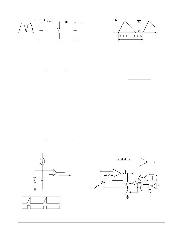
Figure 53. PFC Boost Converter
Figure 54. Inductor Current in DCM
L
I
in
V
in
V
out
Time
Inductor Current
I
pk
T
t
1
t
2
t
3
The NCP1605 operates in voltage mode. As portrayed by
Figure 55, the MOSFET on time t
1
is controlled by the
signal V
ton
generated by the regulation block and the Pin
4 ramp as follows:
t
1
+
C
pin7
@ V
TON
I
pin7
(eq. 2)
The charge current that is sourced by Pin 7
[I
pin7
= 60 mA/V
2
* (V
Pin4
)
2
] is constant at a given input
voltage (V
Pin4
is proportional to the output voltage). C
pin7
that is the capacitor connected between Pin 7 and ground
is also a constant. Hence, the power factor correction is
achieved when the V
TON
(t
1
+ t
2
)/T term is constant.
The output of the regulation block (V
CONTROL
) is
linearly changed into a signal (V
REGUL
) varying between
0 and 1 V. (V
REGUL
) is the voltage that is injected into the
PWM section to modulate the MOSFET dutycycle.
However, like the NCP1601, the NCP1605 inserts some
circuitry that processes (V
REGUL
) to form the signal
(V
TON
) that is used in the PWM section instead of
(V
REGUL
) (see Figure 56). (V
TON
) is modulated in response
to the deadtime sensed during the precedent current
cycles, that is, for a proper shaping of the ac line current
(refer to NCP1601 data sheet). This modulation leads to:
V
TON
+
T @ V
REGUL
t
1
) t
2
or : V
TON
@
t
1
) t
2
T
+ V
REGUL
(eq. 3)
Given the regulation low bandwidth of the PFC systems,
(V
CONTROL
) and then (V
REGUL
) are slow varying signals.
Hence, the (V
TON
* (t
1
+ t
2
)/T) term is substantially
constant. Provided that in addition, (t1) is proportional to
(V
TON
), equation (1) leads to: (I
in
= k * V
in
), where k is a
constant. More exactly:
I
in
+ k @ V
in
(eq. 4)
where : k + constant +
C
pin7
@ V
REGUL
120 m @ L @ (V
pin2
)
2
The input current is then proportional to the input
voltage. Hence, the ac line current is properly shaped.
One can note that this analysis is also valid in the CRM
case. This condition is just a particular case of this
functioning where (t
3
= 0), which leads to (t
1
+ t
2
= T) and
(V
TON
= V
REGUL
). That is why the NCP1605 automatically
adapts to the conditions and jumps from DCM and CRM
(and vice versa) without power factor degradation and
without discontinuity in the power delivery.
Remark: Like in the NCP1601, the
V
TON
processing
circuit
is
informed
when there is an OVP condition, not
to overdimension V
TON
in that conditions. Otherwise, an
OVP sequence would be viewed as a deadtime phase by
the circuit and V
TON
would inappropriately increase to
compensate it.
Similarly, the
V
TON
processing circuit
is inhibited for
a skip sequence not to overdimension
V
TON
in this case
(refer to Figure 56).
Figure 55. PWM Circuit and Timing Diagram
Figure 56. V
TON
Processing Circuit
+
> Vton during (t1+t2)
> 0 V during t3 (deadtime)
> Vton*(t1+t2)/T in average
+
timing capacitor
sawtooth
to PWM latch
PWM
comparator
IN1
S1
S2
C1
R1
SKIP
OVP
OA1
OFF
S3
DT
(high during
deadtime)
The integrator OA1 amplifies the error between V
REGUL
and
IN1 so that in average, (V
TON
*(t1+t2)/T) equates V
REGUL
.
V
REGUL
V
ton
V
ton
Ramp Voltage
PWM Outtage
Turns Off MOSFET
V
ton
C
ramp
I
ch
PWM Comparator
Closed When
Output Low
发布紧急采购,3分钟左右您将得到回复。
相关PDF资料
NCP1606BDR2G
IC POWER FACTOR CONTROLLER 8SOIC
NCP1607BDR2G
IC PFC CONTROLLER CRM 8SOIC
NCP1611BDR2G
IC PFC CTLR HE ENHANCED 8-SOIC
NCP1651DR2G
IC PFC CONTROLLER CCM/DCM 16SOIC
NCP1654BD133R2G
IC PFC CCM 133KHZ 8-SOIC
NCP1927DR2G
IC CTLR PFC/FLYBACK 16-SOIC
NCP380HMU21AATBG
IC CURRENT LIMIT SWITCH 6-UDFN
NCT1008DMT3R2G
TMP DIO MON/SMBUS 4CH 8WDFN
相关代理商/技术参数
NCP1605FORWGEVB
功能描述:电源管理IC开发工具 NCP1605 152 W FORWARD EVB
RoHS:否 制造商:Maxim Integrated 产品:Evaluation Kits 类型:Battery Management 工具用于评估:MAX17710GB 输入电压: 输出电压:1.8 V
NCP1605LCDTVGEVB
功能描述:BOARD EVAL NCP1605/1396 RoHS:是 类别:编程器,开发系统 >> 评估演示板和套件 系列:* 产品培训模块:Obsolescence Mitigation Program 标准包装:1 系列:- 主要目的:电源管理,电池充电器 嵌入式:否 已用 IC / 零件:MAX8903A 主要属性:1 芯锂离子电池 次要属性:状态 LED 已供物品:板
NCP1606ADR2G
功能描述:功率因数校正 IC PWR FCTR CONTROLLER RoHS:否 制造商:Fairchild Semiconductor 开关频率:300 KHz 最大功率耗散: 最大工作温度:+ 125 C 安装风格:SMD/SMT 封装 / 箱体:SOIC-8 封装:Reel
NCP1606APG
功能描述:功率因数校正 IC LO CST PWR FCTR CONT RoHS:否 制造商:Fairchild Semiconductor 开关频率:300 KHz 最大功率耗散: 最大工作温度:+ 125 C 安装风格:SMD/SMT 封装 / 箱体:SOIC-8 封装:Reel
NCP1606BDR2G
功能描述:功率因数校正 IC PWR FCTR CONTROLLER RoHS:否 制造商:Fairchild Semiconductor 开关频率:300 KHz 最大功率耗散: 最大工作温度:+ 125 C 安装风格:SMD/SMT 封装 / 箱体:SOIC-8 封装:Reel
NCP1606BOOSTGEVB
功能描述:电源管理IC开发工具 OSPI NCP1606 100 W BOOST
RoHS:否 制造商:Maxim Integrated 产品:Evaluation Kits 类型:Battery Management 工具用于评估:MAX17710GB 输入电压: 输出电压:1.8 V
NCP1606BPG
功能描述:功率因数校正 IC LO CST PWR FCTR CONT RoHS:否 制造商:Fairchild Semiconductor 开关频率:300 KHz 最大功率耗散: 最大工作温度:+ 125 C 安装风格:SMD/SMT 封装 / 箱体:SOIC-8 封装:Reel
NCP1607BDR2G
功能描述:功率因数校正 IC CST EFCT PW FCTR CTR RoHS:否 制造商:Fairchild Semiconductor 开关频率:300 KHz 最大功率耗散: 最大工作温度:+ 125 C 安装风格:SMD/SMT 封装 / 箱体:SOIC-8 封装:Reel
